ASIC Verification: March 2008

Monday, March 31, 2008

Verilog FAQ1

What are the ways to create a race condition and how can these race conditions can be avoided?

The IEEE Verilog Standard defines which statements have a guaranteed order of execution and which statements don' t have a guaranteed order of execution.

A Verilog race condition occurs when two or more statements that are scheduled to execute in the same simulation time-step, would give different results when the order of statement execution is changed.

module race (out1, out2, clk, rst);
output out1, out2;
input clk, rst;
reg out1, out2;
always @(posedge clk or posedge rst)
if (rst) out1 = 0;
else out1 = out2;

always @(posedge clk or posedge rst)
if (rst) out2 = 1;
else out2 = out1;
endmodule

If the first always block executes first after a reset, both out1 and out2 will take on the value of 1. If the second always block executes first after a reset, both out1 and out2 will take on the value 0. This clearly represents a Verilog race condition.

Making multiple assignments to the same variable from more than one always block is a Verilog race condition, even when using nonblocking assignments.

One of the recommendations is to avoid driving variables from multiple sources.

Illustrate example of how unintentional deadlocked situations can happen during simulation.

The deadlock situation is one in which one process is waiting for the other process to enable it, which in turn will enable the source process. The code could be a syntactically correct implementation, and still have a deadlock situation. The scenario can happen in both synchronous and asynchronous designs. A simple asynchronous example has been illustrated in the following, to demonstrate how deadlock occurs.

module deadlock;
reg reg1, reg2;

initial
begin
reg1 = 1'b0;
wait @ (reg2==1'b1)
end

always @(reg1)
begin
if (reg1==1'b1)
reg2 = 1'b1;
end
endmodule

The above example is an illustration of the deadlock scenario, which can be difficult to capture in a larger implementation.

What is the difference between a vectored and a scalared net?

Both scalared and vectored are Verilog constructs used on multi-bit nets to specify whether or not specifying bit and part select of the nets is permitted. For example,

wire scalared [3:0] a;
wire vectored [3:0] b;

wire c, d;

// Syntax error to use a bit select of vectored net
assign b[1] = 1'b1;
// OK
assign a[1] = 1'b0;

Difference b/w assign, de-assign and force, release.

The assign-deassign and force-release constructs in Verilog have similar effects, but differ in the fact that force-release can be applicable to nets, whereas assign-deassign is applicable only to registers.

The procedural assign-deassign construct is intended to be used for modeling hardware behavior, but the construct is not synthesizable by most logic synthesis tools. The force-release construct is intended for design verification, and is not synthesizable.

What does it mean to “short-circuit” the evaluation of an expression?

Verilog supports numerous operators that have rules of associativity and precedence. In some of the expressions, the result of the expression can be evaluated early on, due to the precedence and influence to override the rest of the expression. In that case, the entire expression need not be evaluated. This is called short-circuiting and expression evaluation.

For example,

assign out = ((a>b) & (c|d));

If the result of (a>b) is false (1'b0), then tools can already determine that the result of the AND operation will be 0. Thus, there is no need to evaluate (c|d) and rest of the equation is short-circuited.


What are the pros and cons of using hierarchical names to refer to Verilog objects?

The top-level module is called the root module because it is not instantiated anywhere. It is the starting point. To assign a unique name to an identifier, start from the top-level module and trace the path along the design hierarchy to the desired identifier.

assign status = top.hub_top.hpie.status_reg;

Adv:
  • It is easy to debug the internal signals of a design, especially if they are not a part of the top level pin out.
Disadv:
  • Sometimes, during synthesis, these hierarchical names get renamed, depending upon the synthesis strategy and switches used, and hence, will cease to exist. In that case, special switches need to be added to the synthesis compiler commands, in order to maintain the hierarchical naming.
  • If the Verilog code needs to be translated into VHDL, the hierarchical names are not translatable.
Does Verilog support an "a to the power b" operator?

Yes. Verilog supports the operation by using two astrices, back to back like,

assign out = (in ** 5);


Sunday, March 30, 2008

Clock Buffer

I read some article about the clock buffer. Clock buffers are designed to have a equal rise and fall times. For designs with global signals, use global clock buffers to take advantage of the low-skew and high-drive strength of the dedicated global buffer tree of the target device. Your synthesis tool automatically inserts a clock buffer whenever an input signal drives a clock signal or whenever an internal clock signal reaches a certain fanout. You can instantiate the clock buffers in your design if you want to specify how the clock buffer resources should be allocated.

Some synthesis tools require you to instantiate a global buffer in your code to use the dedicated routing resource if a clock is driven from a non-dedicated I/O pin. The following Verilog examples instantiate a BUFG for an internal multiplexed clock circuit.

module clock_mux
(
data_in,
sel_in,
slow_clk,
fast_clk,
data_out
);
input data_in, sel_in;
input slow_clock, fast_clock;
output data_out;

reg clock;
wire clock_gbuff;
reg data_out;

always @ (sel_in or fast_clk or slow_clk)
begin
if (sel_in == 1'b1)
clock = fast_clk;
else
clock = slow_clk;
end

buffg gbuff_for_mux
(
.out(clock_gbuff),
.in(clock)
);

always @ (posedge clock_gbuff)
data_out <= data_in;
endmodule

There is an application note from Actel website and can be downloaded from
here.

Saturday, March 29, 2008

Verilog FAQ

What are the differences between blocking and nonblocking assignments?

There is one good paper by Stuart Sutherland about the blocking and non-blocking assignments. This paper can be downloaded from here.


Can you use a Verilog function to define the width of a multi-bit port, wire, or reg type?

The width elements of port declarations require a constant in both MSB and LSB. Before Verilog 2001, it is a syntax error to specify a function call to evaluate the value of these widths. For example, the following code is erroneous before Verilog 2001 version.

reg [ high(val1, val2) : low(val3, value4)] reg1;

In the above example, high and low are both function calls of evaluating a constant result for MSB and LSB respectively. However, Verilog-2001 allows the use of a function call to evaluate the MSB or LSB of a width declaration.

What is the difference b/w the following 2 lines of code?
#5 reg_a = reg_b;
reg_a = #5 reg_b;
Ans: 

Which one is better, asynchronous or synchronous reset for the storage elements?

There is one good paper by Stuart Sutherland about the synchronous and asynchronous reset. This paper can be downloaded from here.

What is the difference b/w the following 2 verilog codes?
a. assign c = condition ? a :b;
b. if(condition) c = a; else c = b;

Ans:


What logic gets synthesized when I use an integer instead of a reg variable as a storage element? Is use of integer recommended?

An integer can take the place of a reg as a storage element. The default width of the integer declaration is 32 bits. If you use integer in your RTL and store a 4 bit value, then the most significant 28 bits will be removed by the optimizer in the synthesis tool in order to minimize the area.

Although the use of integer is a legal construct, it is not recommended for the synthesis of storage elements.


How do you choose between a case statement and a multi-way if-else statement?

A case statement is typically chosen for the following scenarios:
  • When the conditionals are mutually exclusive and only one variable controls the flow in the case statement. The case variable itself could be a concatenation of different signals.
  • To specify the various state transitions of a finite state machine
  • Use of casex and casez allows use of x and z to represent don’t-care bits in the control expression
A multi way if statement is typically chosen in the following scenarios:
  • Synthesizing priority encoded logic
  • When the conditionals are not mutually exclusive
What is the difference between full_case and parallel_case synthesis directive?

There is one good paper by Stuart Sutherland about the full and partial case. This paper can be downloaded from here.

What is the difference b/w casex and casez statements? Which one is preferred?

Ans:
What is delta simulation time?
Ans:

How can you reliably convey control information across clock domains?

The readers are encouraged to read about good design implementation article here.


What are combinatorial timing loops? Why should they be avoided?

Combinatorial timing loops are hardware loops in which the output of either a gate or a long combinatorial path is fed back as an input to the same gate or to another gate earlier in the combinatorial path. These paths are generally created unintentionally when a variable from one combinatorial block is used to drive a signal that is used in the same combinatorial block from which the variable was derived. This typically happens in large size combinatorial blocks, wherein it is difficult to visually track that a loop is getting created.

These combinatorial feedback loops are undesirable for the following reasons:
  • Since there is no clock edge in between to break the path, the combinatorial loops will infinitely keep oscillating and triggering a square waveform, whose duty cycle is dependent upon the sum of ON delays and OFF delays across the combinatorial path.
Combinatorial loops can be caught quite early by one of the following means:
  • Periodic use of linting tools throughout the development process. This is by far the best and easiest way to catch and fix loops early in the design cycle.
  • If the loop is undetected during simulation, many synthesis tools have suitable reporting commands, which detect the presence of a loop. Note that synthesis tools proceed with the static timing analysis by breaking the timing arc of the loop for critical path analysis.

Friday, March 28, 2008

rise and fall time

Consider the dynamic behavior of a CMOS output driving a given capacitvie load. If the resistance of the charging path is double the resistance of the discharging path, is the rise time exatly tiwce the fall time? If not, what other factors affect the transition times?

Design a FF

An CS flip-flop, where C and S are inputs, has the following behavior:
  • If C = 1, the next state is the complement of the current state
  • If C = 0, the next state of the flip-flop is equal to S
Show how to implement an CS flip-flop using a JK flip-flop and logic gates such as NOT, AND, and OR.

Wednesday, March 26, 2008

Multi-cycle path

A Multi-cycle path in a design is a Register-to-Register path, through some combinational logic where if the source register changes, the path will require N number of clock cycles (where N>1) before the computation is propagated to the destination register. It is a good practice for a designer to document these multi cycle paths.


Figure shows path P1 that starts at flip-flop U1, goes through gates G1, G3, G5, and G6, and ends at flip-flop U5. This path has a total propagation delay longer than the clock period for CLK1.

In synthesis, it is encouraged that the designer inform the synthesis tool of any multi-cycle paths. This would allow the synthesis tool to more efficiently optimize the other logic paths that are not meeting the setup requirements rather than to attempt to optimize this multi-cycle path.

To specify this timing exception in STA, use the set_multicycle_path command which has -from, -to, and -through switches. For this example, it would look like this:

set_multicycle_path -from U1 -to U5

False path

In a false path, there is a logical connection from one point to another. Because of the way the logic is designed, this path can never control the timing. For example, a small piece of a design might look like the one in figure.


When select is 0, there's a path from FF1 to FF2 through both multiplexer inputs. Because both selects can never be 0 concurrently (perhaps they are 1 hot signals), this circuit topology will prevent the path from occurring. As a result, this path doesn't need to be optimized to meet the clock cycle timing from the first to the second flip flop. This path is a false one because it can never occur. Even though it is false, a STA tool would flag it as a path. If the delay on the path misses its target, it would flag it as a failing signal. Placing a false-path constraint on this path will allow the synthesis tool to forgo optimizing this path for speed, thereby generating a smaller, lower-power implementation.


Tuesday, March 25, 2008

Who is better Verification Engineer? You or Your Customer?

Why is it that after months of directed and random testing, we were not able to find a bug that our customer found within days of receiving samples? Is there anything wrong with our directed and random testing? Could it be that we didn't run our simulation long enough? Could the bug have been discovered by using better functional coverage?

This article will answers to all those questions by analyzing past mistakes and proposing an effective way of writing a verification plan.

Monday, March 24, 2008

Digital Logic Families

Digital logic families are classified according to the technologies they are built with. Following are the families of digital logic.

  • DL : Diode Logic.
  • RTL : Resistor Transistor Logic.
  • DTL : Diode Transistor Logic.
  • TTL : Transistor Transistor Logic.
  • I2L : Integrated Injection Logic.
  • ECL : Emitter coupled logic.
  • MOS : Metal Oxide Semiconductor Logic (PMOS and NMOS).
  • CMOS : Complementary Metal Oxide Semiconductor Logic.
Among these, only CMOS is most widely used by the ASIC designers; We need to understand a few basic concepts. If you become a ASIC designer, you may need to know these concepts very well.

The most desirable features, a designer would want in IC applications are as follows.
  • Fast switching speed
  • Low power dissipation
  • Wide noise margins
  • High fan-out capability
  • High packing density and
  • Low cost
Although no single family has all these features, some may come close.

Switching Speed

The switching speed of the device is the measured output response to an input change. Typically, a given logic circuit will have many inputs and outputs, with various input to output path and each with a different path delay. Furthermore, switching speed is differ for both low-high and high-low, but both of which are measured from 50% point of the input signal to the 50% point of the output response. Typically tplh > tphl. The maximum value of propagation delay is one of the interest to designers, since it is used to determine useful factors. For the modern CMOS devices, this value lie b/w 0.1 ns to 10 ns.

Power Dissipation

Logic devices consumes power when they operate and this power is dissipated in the form of heat. CMOS power consumption is frequency dependent. Since each gate is connected to the power supply (Vdd). The gate draws certain amount of current during its operation.
  • ICCH - Current drawn during high state
  • ICCL - Current drawn during low state
  • ICCT - Current drawn during transition state
For CMOS, ICCH and ICCL current is negligible, in comparison to ICCT. So the Average power dissipation is calculated as below.

Average Power Dissipation = Vdd * ICCT

So, for CMOS families, the power dissipation depends on the operating frequency. The useful figure of merit for logic devices is called the "Power delay product" and is the multiplication of power consumption and the average tp.

PDP = power_consumption * tp(avg)

Since it is desirable for a given logic device to have a both low power consumption and a small propagation delay (fast switching speed), a low PDP is desirable. Power dissipation is proportional to the heat generated by the chip; Excessive heat dissipation may increase operating temperature and cause gate circuitry to drift out of its normal operating range; It will cause gates to generate improper output values. Thus, power dissipation of any gate implementation must be kept as low as possible. CMOS circuits dissipate power by charging and discharging the various load capacitances (mostly gate and wire capacitance, but also drain and some source capacitances) whenever they are switched. The charge moved is the capacitance multiplied by the voltage change. Multiply by the switching frequency to get the current used, and multiply by voltage again to get the characteristic switching power dissipated by a CMOS device: P = CV2f.

Noise Margin


Noise Margin is the difference between what the driver IC outputs as a valid logic voltage and what the receiver IC expects to see as a valid logic voltage. There are two different types of noise margin, one for a logic high value [1] and one for a logic low value [0]. The equations for noise margins are provided below.


Noise Margin Output high = V
OH [driving device] - VIH [receiving device]
Noise Margin Output low = VIL [receiving device] - VOL [driving device]

The higher the numbers the better, with negative numbers indicating in-operability.

Fan In

Fan-in is the number of inputs a gate has, like a two input AND gate has fan-in of two, a three input NAND gate as a fan-in of three. So a NOT gate always has a fan-in of one. The figure below shows the effect of fan-in on the delay offered by a gate for a CMOS based gate. Normally delay increases following a quadratic function of fan-in.

Fan Out

The number of gates that each gate can drive, while providing voltage levels in the guaranteed range, is called fan-out. The fan-out depends on the amount of electric current a gate can source or sink while driving other gates. The effects of loading a logic gate output with more than its rated fan-out has the following effects.
  • In the LOW state, the output voltage VOL may increase above VOLmax.
  • In the HIGH state, the output voltage VOH may decrease below VOHmin.
  • The operating temperature of the device may increase thereby reducing the reliability of the device and eventually causing the device failure
  • Output rise and fall times may increase beyond specifications
  • The propagation delay may rise above the specified value

Sunday, March 23, 2008

Multiplexing the clock

In today's VLSI industry, we are working on multi-clock domain all the time. In that case, we are often encountered to switch the functional clocks while the chip is running. This is generally implemented by multiplexing the two different clocks with select signal is generated from the internal logic.

The two clock frequencies could be totally asynchronous to each other or they may be multiples of each other. In either case, there is a chance of generating a 'glitch' on the clock line at the time of the switch. A glitch on the clock line is hazardous to the whole system, as it could be interpreted as a capture clock edge by some registers while missed by others.

But designing glitch free clock multiplexing is a tricky one. Some designers take it on the safer side by disabling both clocks, change the select signal and enable the clocks.

In this article, two different methods of designing a glitch free clock multiplexing are presented. The first method is used when clocks are multiples of each other, while the second method deals with clocks which are totally unrelated to each other.

Saturday, March 22, 2008

Arrange the 4 n-bit numbers

There is a component called "X" with 2 inputs - A and B, and 2 outputs - X and Y. If you pass 2 n-bit numbers to the component X, the component produced the biggest number at the output X and the smallest number at the output Y.

Using minimum numbers of these components "X", Design a component "M" with 4 inputs A, B, C and D and 4 outputs W, X, Y and Z in which

'W' is the max (A, B, C, D), 'Z' is the min(A, B, C, D). 'X' is bigger than 'Y' but smaller than 'W' and 'Y' is bigger than 'Z' and smaller than 'X'.


Equation for ppm

Given an Ideal Frequency (f) and its uncertainty is given as plus or minus delta-f. Find the accuracy in parts per million (ppm) using f and delta-f.

Wednesday, March 19, 2008

Gate level simulation - Part 2

Gate level simulation is used in the late design cycle to increase the level of confidence about a design implementation and can help to verify dynamic circuit behavior that cannot be accurately verified with static methods. For example the start up and reset phase of a chip. To reduce the overall cycle time, only a minimum amount of vectors should be simulated using the most accurate timing model available.

Unit delay simulation

The net list after synthesis, but before routing does not contain the clock tree. It does not make sense to use SDF back annotation at this step, but GLS may be used to verify the reset circuit, the scan chain or to get data for power estimation. If no back annotation is used, simulators should use libraries which have the specified block containing timing arcs disabled and using Distributed delays instead.

Full timing simulation with SDF

Simulation is run by taking full timing delays from SDF. The SDF file is used to back annotate values for propagation delays and timing checks to the Verilog gate level net list.

Timing 1

Due to a miscommunication during design, you thought your circuit was supposed to have a supply voltage of 2.1 volts and a 25 ns cycle time, and you designed it to meet those specifications. Now your boss tells you, you were supposed to have a 20 ns cycle time. To avoid redesigning the whole circuit, your co-worker suggests increasing the voltage of the circuit to decrease the delay to 20 ns. The same co-worker also suggests picking some arbitrary number like 3.5 volts.

  1. Determine the new cycle time of your circuit with a 3.5 volt input voltage.
  2. Calculate the increase in power consumption of your circuit at 3.5 volts.
  3. To satisfy your boss, calculate the minimum voltage you would increase the supply voltage to, in order to allow your circuit to run at 20 ns.
You may leave your answer in non-simplified numeric terms, but not in the form of an equation to solve.

STA question 1

Suppose we are building the following circuit using only three components:

  • Inverter: tcd = 0.5ns, tpd = 1.0ns, tr = tf = 0.7ns
  • 2-input NAND: tcd = 0.5ns, tpd = 2.0ns, tr = tf = 1.2ns
  • 2-input NOR: tcd = 0.5ns, tpd = 2.0ns, tr = tf = 1.2ns
What is tpd (Propagation delay) for this circuit?
What is tcd (Contamination delay) for this circuit?

What is tpd of the fastest equivalent circuit built using only above 3 components?

Hint:
tpd - Max. cumulative propagation delay considering all path b/w input and output.
tcd - Min. cumulative contamination delay.


Gate level simulation

Even though a lot of STA and Formal verification tools exists in the industry now a days, one question still arises in the mind of many verification engineers. The question is "Why do we go for a gate level simulation?"

Some years ago, I felt that gate level simulation were not worth. In my view, if we do static timing analysis (STA) - Those who want to know more about STA, please click here - after post and route, and take the post routed net-list, Extracted Parasitics File and design timing constraints, then perform design timing checks at all corners - say setup, hold and clock gating check - then we should be OK, no need to perform the gate level simulation. Then I realized if our chip has system clocks that only talk to others in synchronous, works in a single mode of operation and the STA setup includes no constants and false paths, then we can cover everything through STA tools.

Gate level simulation represents a small slice of what should actually be tested for a tape-out. They offer a warm feeling that, what you are going to get back will actually work and secondly, they offer some confidence that your static timing constraints are correct.

But the common reason to go for a gate level simulations are as follows:

  • To check if the reset release, initialization sequence and boot up sequences are proper.
  • STA tools doesn't verify the asynchronous interfaces.
  • Unintended dependencies on initial conditions can be found through GLS
  • Good for verifying the functionality and timing of circuits and paths that are not covered by STA tools
  • Design changes can lead to incorrect false path/multi cycle path in the design constraints.
  • It gives an excellent feeling that the design is implemented correctly

So before shipping a design to tape-out, we run a limited set of gate level simulations. Because there are some difficulties associated with this GLS, they are:

  • Takes a lot of setting up and debugging
  • Takes a huge amount of computing recourses ( CPU time and disk space for storing wave)
  • RTL simulations alone take multiple days of run time even for a single regression. GLS takes 10* times.
  • Generation of debug data (VCD, Debussy) is impossible with GLS

Some design teams use GLS only in a zero-delay, ideal clock mode to check that the design can come out of reset cleanly or that the test structures have been inserted properly. Other teams do fully back annotated simulation as a way to check that the static timing constraints have been set up correctly.

In all cases, getting a gate level simulation up and running is generally accompanied by a series of challenges so frustrating that they precipitate a shower of adjectives as caustic as those typically directed at your most unreliable internet service provider. There are many sources of trouble in gate level simulation. This series will look at examples of problems that can come from your library vendor, problems that come from the design, and problems that can come from synthesis. It will also look at some of the additional challenges that arise when running gate level simulation with back annotated SDF.

So In my opinion, the gate-level simulations are needed mainly to verify any environment and initialization issues.

Thursday, March 13, 2008

Hands on Training in Specman - 2

Today is the last day of our Specman Tutorial. The previous section explains the complete verification process of a simple USB packet ID decoder design. Topics discussed are design specification, verification components, verification plan, and test plan. This section completes the example with an explanation of the actual 'e' code for each component required for the verification of the PID Decoder design.

Defining the packet data item

This section shows the 'e' code for the packet data item.

//==========================================================================

<'
-- Define an enumerated type packet_id.
-- The token type is either IN, OUT or SETUP

type
packet_id : [IN, OUT, SETUP, ERR_PID];

-- Define a struct called hub_packet

struct hub_packet
{

-- Define a field syn; The value of sync field is constant

%syn : uint(bits:32);
-- SYNC pattern is 32'h8000_000;
keep soft syn == 32'h8000_0000;
--Define a field pid
%pid : packet_id;

pid_type : uint(bits:8);
-- Endpoint Number
%ep_no : uint(bits:4);
keep soft ep_no in [1..15]; -- Device address
%dev_add : uint(bits:7);

keep soft dev_add == 10;
%data : list of uint(bits:16); -- Packet length pid=8bits; dev_add=7bits; ep_nu=4bits;
keep pid == IN => pid_type == 8'h69;

keep pid == OUT => pid_type == 8'hE1;

keep pid == SETUP => pid_type == 8'h2D;
keep pid == ERR_PID => pid_type == 8'h11;
// Pid error
%crc_5 : uint(bits:5);

keep crc_5 == 5'b10101;

// Keep the CRC fixed as of now
%eop : byte;
keep soft eop == 8'hFE;

event coverage_chk;

};

extend sys
{
packets : list of hub_packet;
keep packets.size() == 2;
};
// End of extend
'>
//==========================================================================

Defining the Transaction Generator

This section shows the 'e' code for the Transaction generator.
//==========================================================================
-- Transaction Generator
//==========================================================================

<'
import hub_packet;
import hub_driver;
unit hub_txgen
{
// Instantiate the struct hub_packet, the static verification object
hub_object : hub_packet;

// Instantiate the unit hub_driver, the dynamic verification object
hub_driver : hub_driver is instance;
keep hub_driver.hdl_path() == "~/pid_dec_TB";

// Define a positive edge of the clock
event posedge_clk is rise('pid_dec_TB.clock_in') @sim;

// Define a TCM, gen_transaction which will start another TCM
gen_transaction()@ posedge_clk is
{
// Start to generate and drive the USB packet
start hub_driver.gen_and_drive();
};
// End of gen_transaction
};
// End of unit
'>
//==========================================================================

Defining the Hub driver

This section shows the 'e' code for the hub driver.
//==========================================================================
// Hub Driver
//==========================================================================
<'
import hub_packet;
-- import the hub_packet here

unit hub_driver
{
!current_packet : hub_packet;
!delay : uint;
keep soft delay in [1..10];
no_of_packets : uint;

event rise_clk is rise ('clock_in') @sim;
event fall_reset is fall ('reset_in') @sim;
event sync_on_bus;
event pid_on_bus;
event packet_ended;

sent_signals() @rise_clk is
{
'rx_last_byte' = 0;
'rx_bs_err' = 0;
'rx_valid' = 0;

wait @sync_on_bus;
'rx_valid' = 1;

wait @pid_on_bus;
'rx_last_byte' = 1;
'rx_valid' = 1;

wait;
'rx_last_byte' = 0;
'rx_bs_err' = 0;
'rx_valid' = 0;
};
// End of sent_signals() method

gen_and_drive () @ rise_clk is
{
for i from 0 to no_of_packets-1
{
gen delay;
wait [delay];
gen current_packet;

wait true ('reset_in' == 0);
drive_packet (current_packet);
};
-- end of for loop
};
-- end of generate_and_drive method

drive_packet (packet : hub_packet) @rise_clk is
{
var packet_packed : list of uint(bits:16);
emit packet.coverage_chk;

packet_packed = pack (packing.low, packet.syn[15:0], packet.syn[31:16], packet.ep_no[0:0], packet.dev_add[6:0], packet.pid_type, packet.crc_5, packet.ep_no[3:1],packet.eop);

for each
(packet_16bit) in packet_packed
{
'data_in' = packet_16bit;
start sent_signals();
wait cycle;

if('data_in' == 16'h8000)
{
emit sync_on_bus;
};

if('data_in'[15:8] == 8'h69 || 'data_in'[15:8] == 8'hE1 || 'data_in'[15:8] == 8'h2D || 'data_in'[15:8] == 8'h11)
{
emit pid_on_bus;
};
};
emit packet_ended;
};
-- end drive_packet
};
'>
//==========================================================================

Defining the hub output monitor

This section shows the 'e' code for the hub's output monitor.
//==========================================================================
// Hub output monitor
//==========================================================================
<'
import hub_env;
unit hub_op_mon
{
!rcv_packet : hub_packet;
rcv_delay : uint;

keep soft rcv_delay == 10;

event posedge_clk is rise ('clock_in') @sim;
event in_token_rcvd is rise ('in_token_out')@ posedge_clk;
event out_token_rcvd is rise ('out_token_out')@ posedge_clk;
event setup_token_rcvd is rise ('setup_token_out')@ posedge_clk;

output_mon() @ posedge_clk is
{
while(TRUE)
{
wait cycle;
if(('in_token_out' == 1 ) || ('out_token_out' == 1) || ('setup_token_out' == 1) || ('pid_error_out' == 1) )
{
if('in_token_out' == 1) then
{
out("IN TOKEN RECEIVED SUCCESSFULLY at ", sys.time);
}
else if ('out_token_out' == 1) then
{
out("OUT TOKEN RECEIVED SUCCESSFULLY at ", sys.time);
}
else if('setup_token_out') then
{
out("SETUP TOKEN RECEIVED SUCCESSFULLY at ", sys.time);
}
else
{
out("PID Error is Occured at ", sys.time); };};};};};
'>
//==========================================================================

Defining the coverage item

This section shows the 'e' code for the coverage item.
//==========================================================================
// Coverage
//==========================================================================
<'
import
hub_env;
import
hub_packet;

extend
hub_packet
{
cover coverage_chk using
count_only,
radix = HEX,
weight = 10 is
{
item pid;
item
ep_no;
cross
pid, ep_no;
};
// End of cover
};
// End of extend
'>
//==========================================================================

Defining the Top level hierarchy


This section shows the 'e' code for the top level verification hierarchy.
//==========================================================================
-- Top level of 'e' verification hierarchy
//==========================================================================

<'
import
hub_packet;
import hub_driver;
import tx_gen;
import hub_cover;
import hub_output_mon;

unit hub_env
{
-- Instantiate hub_tx_gen
hub_tx_gen : hub_txgen is instance;

// Instantiate hub_driver

hub_driver : hub_driver is instance;
keep hub_driver.hdl_path() == "~/pid_dec_TB";

-- Instantiate hub_output_monitor
hub_op_monitor : hub_op_mon is instance;
keep hub_op_monitor.hdl_path() == "~/pid_dec_TB";

event posedge_clk is rise('pid_dec_TB.clock_in') @sim;

// Define a TCM, start_tb which will start all the TCMs
start_tb() @ posedge_clk is
{
start hub_op_monitor.output_mon();
// start output mon
start hub_tx_gen.gen_transaction();
// start method

wait[1200];
stop_run();
// call method
};
// End of start_tb()
};
// End of unit

-- Create an instance of hub_env object in top level
extend sys
{
hub_env : hub_env is instance;
run() is also
{
start hub_env.start_tb();
};
// End of run()
};
// End of extend

extend sys
{
setup() is also
{
set_config( print, scale, ps);
set_config( cover, mode, on);
};
// End of setup()
};
// End of extend

'>
//==========================================================================

Test case 1

This section shows the 'e' code for the test case.
//==========================================================================
//Test

//==========================================================================
<'
import
hub_env;

extend hub_packet
{


keep soft dev_add in [1..10];

keep soft pid == select
{
20: [IN];
30: [OUT];
20: [SETUP];
20: [ERR_PID];
};

extend sys
{
keep hub_env.hub_driver.no_of_packets == 5 ;
};
'>
//==========================================================================

Procedure to run the test case

Create the simulation directory
mkdir sim

Go to the simulation directory
cd sim

Create the work library
vlib work


Create the stubs file in hdl directory
$SPECMAN_HOME -command "write stubs -verilog ../hdl/specman.v"


Compile the stubs and design files
vlog -work ./work ../hdl/specman.v
vlog -wrok ./work ../hdl/pid_dec.v
vlog -wrok ./work ../hdl/pid_dec_TB.v

Run the simulation
Invoking Specman and Modelsim
$SPECMAN_HOME../sn/bin/specview -p "load ../e/test1; test" vsim -pli ../../libmti_sn_boot.so -lib ./work pid_dec_TB &

//==========================================================================


Wednesday, March 12, 2008

Hands on Training in Specman - 1

In the previous sections, we focussed mainly on introductory and syntax aspects of 'e'. However, it is important for a verification engineer to understand how to build a complete verification system with 'e'. This section discusses the complete verification process of a simple USB packet's pid decoder. This section also discusses the specification of USB's packet ID decoder, verification components, verification plan and test plan.

DUT Specification

This section describes the complete DUT specification of a simple USB packet ID decoder. Figure shows the input/output specification of the DUT. The PID Decoder accepts data packet on a single 8-bit input port called 'data_in' and in combination with the transceiver signals - rxvalid, rxlastbyte and rxbserror - it decodes the packet ID.

Data Packet Description


A token packet is a sequence of bytes with first 4 bytes containing sync field, the next set of bytes containing data and the last byte containing CRC. The packet format has the following characteristics.
  • The 'SYNC' consists of 32 bits - 32'h8000_0000 ( The LSB is transmitted first)
  • PID is 8 bits. The first 4 bits are 'type' field and the next 4 bits are compliment of 'type'
  • Address is 7 bits.
  • Endpoint is 4 bits.
  • CRC5 is 5 bits
All packets begin with a synchronization (SYNC) field. A SYNC from an initial transmitter is defined to be 32 bits for high-speed. SYNC serves only as a synchronization mechanism. The last two bits in the SYNC field are a marker that is used to identify the end of the SYNC field and the start of the PID.

A packet identifier (PID) immediately follows the SYNC field of every USB packet. A PID consists of a four-bit packet type field followed by a four-bit check field. The PID indicates the type of packet. The four-bit check field of the PID ensures reliable decoding of the PID so that the remainder of the packet is interpreted correctly. The PID check field is generated by performing a one' s complement of the packet type field. A PID error exists if the four PID check bits are not complements of their respective packet identifier bits.

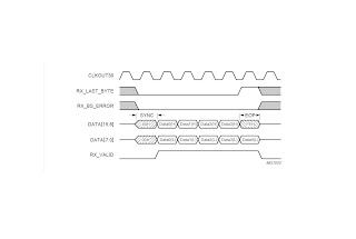
DUT Input Protocol

Figure shows the input protocol of the DUT. The characteristics of the DUT input protocol are as follows:

  • All input signals are active high and are synchronized to the rising edge of the clock. Therefore, any signal that is an input to the DUT is driven at the rising edge of the clock.
  • The rx_valid signal has to be asserted on the same clock after the sync packet is transmitted.
  • The rx_last_byte signal has to be asserted if the EOP is on the higher order byte and valid data is on the lower order byte.

DUT Output Protocol

Figure shows the output protocol of DUT. The characteristics of the DUT output protocol are as follows:

  • All output signals are active high and are synchronized to the rising edge of the clock. Therefore, any signal that is an output from the DUT is sampled at the rising edge of the clock.
  • The Decoder asserts the 'in_token' when it detects '69' in the 'PID' field & the edge of rx_valid signal.
  • The Decoder asserts the 'out_token' when it detects 'E1' in the 'PID' field & the edge of rx_valid signal.
  • The Decoder asserts the 'setup_token' when it detects '2D' in the 'PID' field & the edge of rx_valid signal.
  • The Decoder asserts the 'pid_err_out' when 'type' field and its compliment doesn't match & the edge of rx_valid signal.

DUT HDL Source Code

Example shows the verilog source code used to describe the DUT PID Decoder.


//***************************************************************************************************************
// Block : pid_dec
// Description : This block decodes the pid and asserts the corresponding
// tokens and also asserts the pid error if the last four bits
// are not the compliment of the first four bits
//***************************************************************************************************************
module pid_dec
(

// Inputs

clock_in,
reset_in,

rx_valid,
rx_last_byte,
rx_bs_err,
data_in,

// Outputs

in_token_out,
out_token_out,
setup_token_out,
pid_error_out,
invalid_token_out
);


// Inputs

input clock_in;
input reset_in;
input[15:0] data_in;

input rx_valid;
input rx_last_byte;
input rx_bs_err;

// Outputs

output in_token_out;
output out_token_out;
output setup_token_out;
output invalid_token_out;
output pid_error_out;

reg in_token_out;
reg out_token_out;
reg setup_token_out;
reg invalid_token_out;
reg pid_error_out;


// Signal Declarations

reg next_in;
reg next_out;
reg next_setup;
reg next_invalid;
reg next_pid_err;
reg rx_valid_r;

wire rx_valid_edge;


assign rx_valid_edge = rx_valid & ~rx_valid_r;

// Signal Assignments .


//***************************************************************************************************************
// Process for PID Decode
//***************************************************************************************************************
always @(data_in)
begin : hpdc_main
next_in = 1'b0 ;
next_out = 1'b0 ;
next_setup = 1'b0 ;
next_invalid = 1'b0 ;
next_pid_err = 1'b0 ;

// Here last four bits are taken and compared with its
// compliment inorder to verify whether the pid and
// its complement are proper

case (data_in[11:8])
4'b0001 :
// Decoding OUT PID
begin
if ((data_in[15:12] == ~(data_in[11:8])) && rx_valid_edge)
begin
next_out = 1'b1 ;
next_pid_err = 1'b0 ;
end
else if ((data_in[15:12] != ~(data_in[11:8])) && rx_valid_edge)
begin
next_pid_err = 1'b1 ;
end
else
next_pid_err = 1'b0 ;

end

4'b1001 :
// Decoding IN PID
begin
if ((data_in[15:12] == ~(data_in[11:8])) && rx_valid_edge)
begin
next_in = 1'b1 ;
next_pid_err = 1'b0 ;
end
else if ((data_in[15:12] != ~(data_in[11:8])) && rx_valid_edge)
begin
next_pid_err = 1'b1 ;
end
else
next_pid_err = 1'b0 ;
end
4'b1101 :
// Decoding SETUP PID
begin
if ((data_in[15:12] == ~(data_in[11:8])) && rx_valid_edge)
begin
next_setup = 1'b1 ;
next_pid_err = 1'b0 ;
end
else if ((data_in[15:12] != ~(data_in[11:8])) && rx_valid_edge)
begin
next_pid_err = 1'b1 ;
end
else
next_pid_err = 1'b0 ;
end

// Incase the incoming bit stream contains anything other than
// the expected value then this default state is entered

default :
begin
next_invalid = 1'b1 ;
end
endcase
end


//***************************************************************************************************************
// Process for latching the Decoded PID
//***************************************************************************************************************
always @(negedge reset_in or posedge clock_in)
begin : hpdc_regs
if (reset_in)
begin
in_token_out <= 1'b0 ;
out_token_out <= 1'b0 ;
setup_token_out <= 1'b0 ;
invalid_token_out <= 1'b0 ;
pid_error_out <= 1'b0 ;
rx_valid_r <= 1'b0;
end
else
begin
begin
in_token_out <= next_in ;
out_token_out <= next_out ;
setup_token_out <= next_setup ;
invalid_token_out <= next_invalid ;
pid_error_out <= next_pid_err ;
rx_valid_r <= rx_valid;
end
end
end
endmodule

Test bench

module pid_dec_TB;

reg clock_in;
reg reset_in;


reg [15:0] data_in;

reg rx_valid;
reg rx_last_byte;
reg rx_bs_err;
wire in_token_out;
wire out_token_out;
wire setup_token_out;
wire pid_error_out;
wire invalid_token_out;


pid_dec inst_pid_dec
(

.clock_in(clock_in),
.reset_in(reset_in),
.data_in(data_in),
.rx_valid(rx_valid),
.rx_last_byte(rx_last_byte),
.rx_bs_err(rx_bs_err),
.in_token_out(in_token_out),
.out_token_out(out_token_out),
.setup_token_out(setup_token_out),
.pid_error_out(pid_error_out),
.invalid_token_out(invalid_token_out)
);


specman sn();

// clock_in generation logic

initial
begin
clock_in = 1'b0;
reset_in = 1'b1;
forever
#5 clock_in = ~clock_in;

end

initial
begin
#100 reset_in = 1'b0;
end

endmodule // pid_dec_TB


Verification Plan

A verification plan is required to describe what is to be verified and how it will be verified. It also should address 3 aspects of verification.

  1. Coverage measuresment
  2. Stimulus Generation
  3. Response Checking

The verification will be developed in 'e'.

Test Plan

Tests are derived from test plan. A test plan contains all tests that are to be run to verify the DUT. A test plan contains an exhaustive list of items to be tested. In 'e' tests are simply the extensions of existing structs and unit definitions.

Test1

Create the packets with a certain probability distribution.